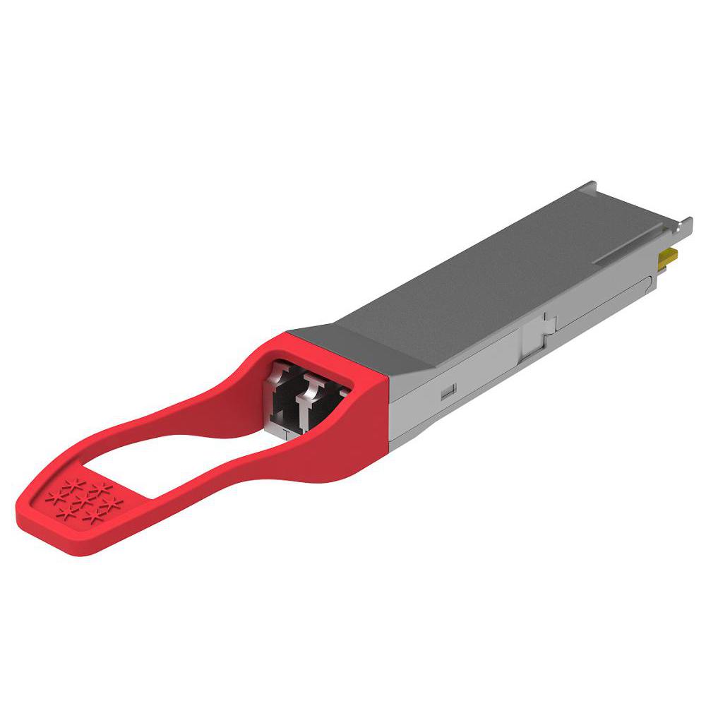
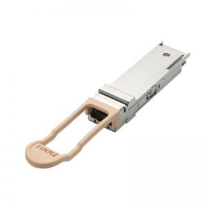
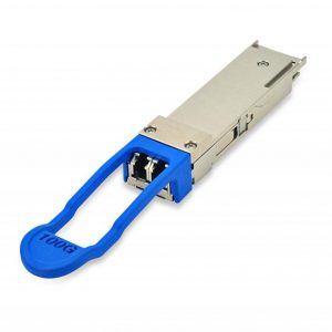
FYQ28-31R4-40BD 100Gb/s QSFP28 ER4 Lite Transceiver
Description
PRODUCT FEATURES
- Compliant with 100GBASE-ER4
- Support line rates from 103.125 Gbps to 111.81 Gbps
- Integrated LAN WDM TOSA / APD ROSA for up to 30 km reach over SMF without FEC
- Digital Diagnostics Monitoring Interface
- Duplex LC optical receptacle
- No external reference clock
- Electrically hot-pluggable
- Compliant with QSFP28 MSA with LC connector
- Case operating temperature range:0°C to 70°C
- Power dissipation < 4.0 W
APPLICATIONS
- 100G Ethernet &100GBASE-ER4
- ITU-T OTU4
STANDARD
- Compliant to IEEE 802.3ba ,IEEE 802.3bm and 100G ER4
- Compliant to SFF-8636
General Description
FlyinFiber 100G QSFP28 ER4 Lite optical Transceiver integrates receiver and transmitter path on one module. In the transmit side, four lanes of serial data streams are recovered, retimed, and passed to four laser drivers. The laser drivers control 4- EML with center wavelength of 1296 nm, 1300nm, 1305nm and 1309 nm. The optical signals are multiplexed to a single –mode fiber through an industry standard LC connector. In the receive side, the four lanes of optical data streams are optically de-multiplexed by the integrated optical de- multiplexer. Each data stream is recovered by a APD and trans-impedance amplifier, retimed. This module features a hot-pluggable electrical interface, low power consumption and MDIO management interface.
The product is designed with form factor, optical/electrical connection and digital diagnostic interface according to the QSFP28 Multi-Source Agreement (MSA) and compliant to IEEE 802.3bm.


Notes:
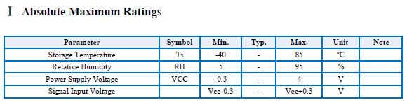
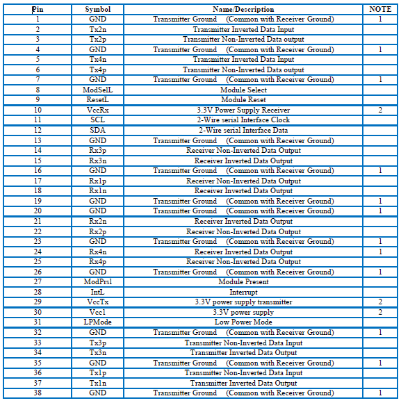
- GND is the symbol for signal and supply (power) common for QSFP28 modules. All are common within the QSFP28 module and all module voltages are referenced to this potential unless otherwise noted. Connect these directly to the host board signal common ground plane.
- VccRx, Vcc1 and VccTx are the receiving and transmission power suppliers and shall be applied
concurrently. Recommended host board power supply filtering is shown below. Vcc Rx, Vcc1 and Vcc Tx may be internally connected within the QSFP28 transceiver module in any combination. The connector pins are each rated for a maximum current of 500mA.
VI. Digital Diagnostic Functions
FlyinFiber FYQ28-31R4-40BD support the 2-wire serial communication protocol as defined in the QSFP28 MSA. Which allows real-time access to the following operating parameters:
- Transceiver temperature
- Laser bias current
- Transmitted optical power
- Received optical power
- Transceiver supply voltage
It also provides a sophisticated system of alarm and warning flags, which may be used to alert end- users when particular operating parameters are outside of a factory-set normal range.
The operating and diagnostics information is monitored and reported by a Digital Diagnostics Transceiver Controller inside the transceiver, which is accessed through the 2-wire serial interface. When the serial protocol is activated, the serial clock signal (SCL pin) is generated by the host. The positive edge clocks data into the QSFP28 transceiver into those segments of its memory map that are not write-protected. The negative edge clocks data from the QSFP28 transceiver. The serial data signal (SDA pin) is bi- directional for serial data transfer. The host uses SDA in conjunction with SCL to mark the start and end of serial protocol activation. The memories are organized as a series of 8-bit data words that can be addressed individually or sequentially. The 2-wire serial interface provides sequential or random access to the 8 bit parameters, addressed from 00h to the maximum address of the memory.
This clause defines the Memory Map for QSFP28 transceiver used for serial ID, digital monitoring and certain control functions. The interface is mandatory for all QSFP28 devices. The memory map has been changed in order to accommodate 4 optical channels and limit the required memory space. The structure of the memory is shown in Figure 2 -QSFP28 Memory Map. The memory space is arranged into a lower, single page, address space of 128 bytes and multiple upper address space pages. This structure permits timely access to addresses in the lower page, e.g. Interrupt Flags and Monitors. Less time critical entries, e.g. serial ID information and threshold settings, are available with the Page Select function. The structure also provides address expansion by adding additional upper pages as needed. For example, in Figure 2 upper pages 01 and 02 are optional. Upper page 01 allows implementation of Application Select Table, and upper page 02 provides user read/write space. The lower page and upper pages 00 and 03 are always implemented. The interface address used is A0xh and is mainly used for time critical data like interrupt handling in order to enable a “one-time-read” for all data related to an interrupt situation. After an Interrupt, IntL, has been asserted, the host can read out the flag field to determine the effected channel and type of flag.
For more detailed information including memory map definitions, please see the QSFP28 MSA Specification.
VII. Host – Transceiver Interface Block Diagram

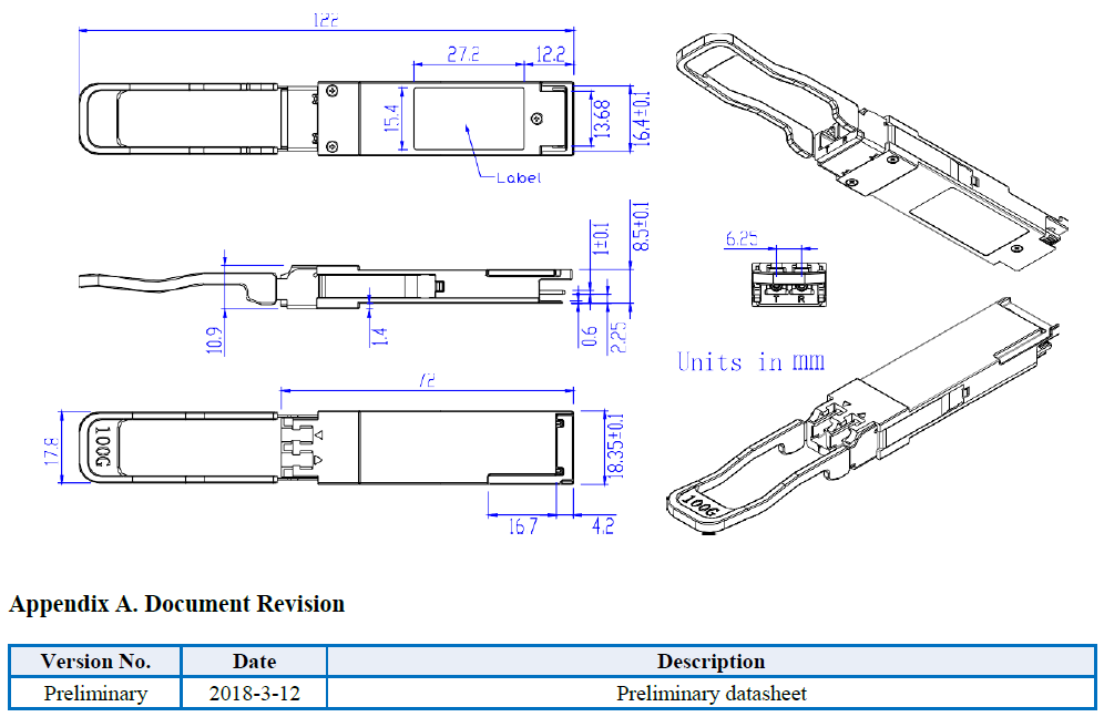
VIII. Outline Dimensions
Only logged in customers who have purchased this product may leave a review.
Reviews
There are no reviews yet.